Oculus2: Storage
Oculus 2 uses iNAND flash with interface UFS and sizes of 64GB, 128GB, or 256 GB. I saw a 32GB mainboard on eBay but did not see an official announcement of such a size.
Part number is WDC SDINDDH4-xxG. Package VFBGA-153
I was not able to find the datasheet for these parts, but I found an example of a pinout for UFS 3.1 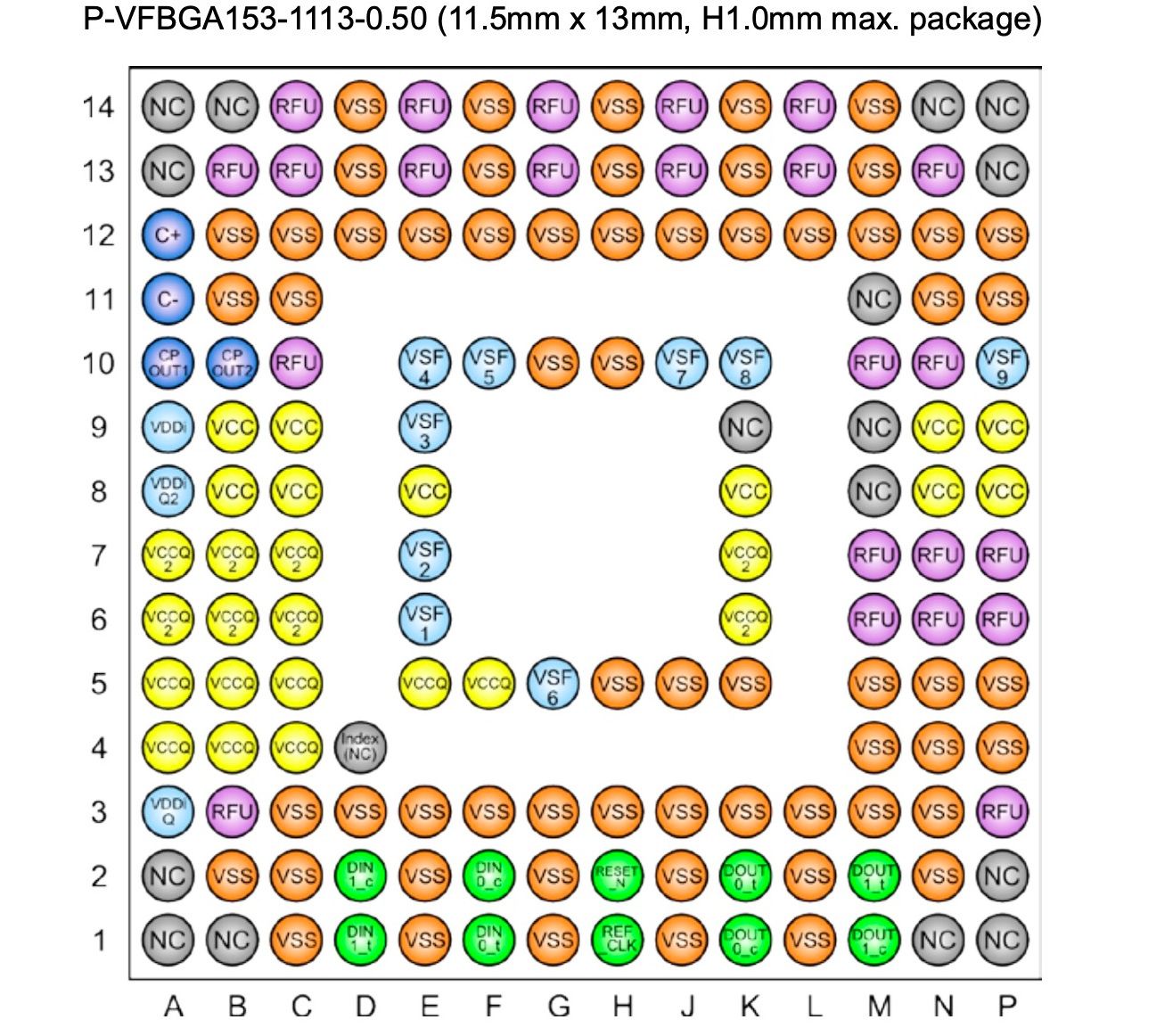
Pinout description: 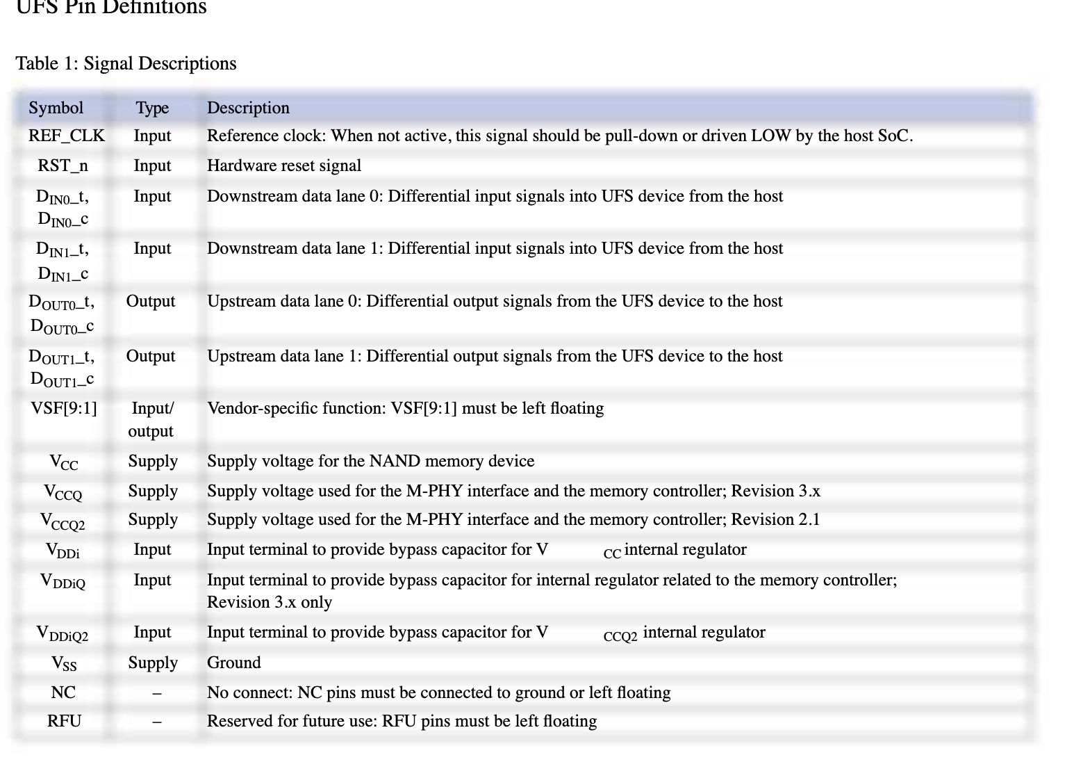
Also, I tried to find a way to dump or re-write a flash without desoldering the IC but unfortunately looks like DIN/DOUT lines go directly to SoC which is understandable because they are differential lines. Corresponding UFS pins on the flash and SoC ICs: 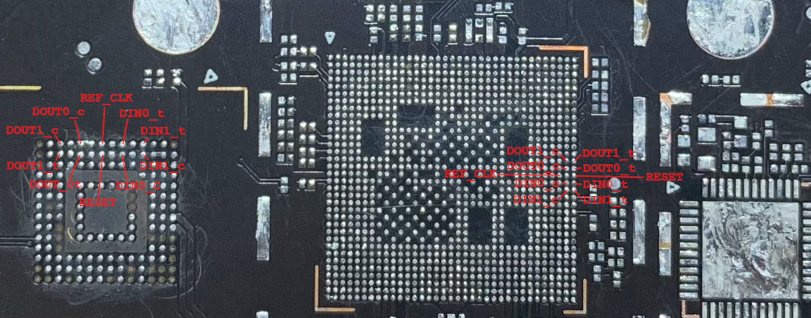
UFS pins are on the SoC side, so theoretically, it may be possible to remove a packaging compound from this side and solder wires (wires should be the same length, of course) directly to SoC pins, but it is too complicated for me (at least for now).
Another option is to design an adapter for UFS flash with access to these pins and to solder it instead of the flash. For now, I dumped the entire content of the flash using the “Medusa PRO II Box” tool. This tool works great with UFS flash, but the software is a nightmare (maybe I will write a separate post about it).