Oculus2: Unlocking Secrets: A Journey into Firmware Extraction from the Controller
Intro
As we found out in Oculus2: Inside the Controller, a controller is based on nRF52832 SoC.
Nordic Semiconductor nRF52832 Multiprotocol BLUETOOTH® 5.2 SoCs are powerful and highly flexible, making them ideal for BLUETOOTH Low Energy, ANT, and 2.4GHz ultralow-power wireless applications. Nordic nRF52832 SoCs are built around a 32-bit Arm® Cortex®-M4F CPU with 512kB + 64kB RAM. The embedded 2.4GHz transceiver supports BLUETOOTH Low Energy, ANT, and a proprietary 2.4 GHz protocol stack.
The nrf52 series lacks a verified boot feature but offers the APPROTECT feature to secure content. The sole method to turn off this protection is by performing an ERASEALL on the SoC.
In 2020, LimitedResults found a method to deactivate APPROTECT and successfully dump firmware. Originally, this was made for nrf52840 and then scaled to other SoC from this family:
- nRF52 Debug Resurrection (APPROTECT Bypass) Part 1
- nRF52 Debug Resurrection (APPROTECT Bypass) Part 2
Since this discovery, numerous individuals have started exploring this domain to acquire hands-on experience:
- ESP32_nRF52_SWD
- APPLE AIRTAGS HACKED AND CLONED WITH VOLTAGE GLITCHING
- Apple AirTag Teardown & Test Point Mapping
- and others
Background
This section provides a brief background on the attack, originally detailed in the blog post by LimitedResults. If you’re already familiar with it, you may skip this part.
Overview
Typically, an external debugger is accessing the ARM CPU through the Debug Access Port (DAP). Then, two different ports are available:
- CTRL-AP. This is the Master Debug Port, and it is not dependent on APPROTECT. It will be used to recover, in case of a bricked device, for example
- AHB-AP. This is the real Debug Port to access memories and control the CPU via SWD.
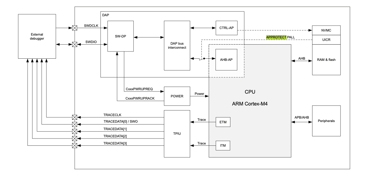
The Boot Process is relatively simple due to the fact that the nRF52840 does not contain boot ROM code.
All the blocks, like the NVMC, the memories, the Debug Acces Port, etc, are initialized purely in Hardware. After a Power-on Reset, the AHB-AP has to initialize itself according to the value of the APPROTECT, which is stored in UICR (a dedicated Flash memory partition).
During the boot, the Memory Controller (NVMC) has to communicate with the CPU (or with the AHB-AP Block directly) to provide the APPROTECT value stored in Flash, and then set its protection state accordingly.
Due to the absence of BootROM, this is achieved by pure Hardware, and it has to be done during the early boot process before the CPU starts to load from Flash and execute Code.
The goal is to identify this “pure HW process” and then try to modify the AHB-AP Debug Initialisation. If successful, the Debug features will be reactivated until the next Power-on Reset.
Power configuration
The system contains two different regulator stages, REG0 and REG1. Each regulator stage has two different configurable options based on Low-dropout Regulators (LDO) and Buck Regulators (DC/DC). 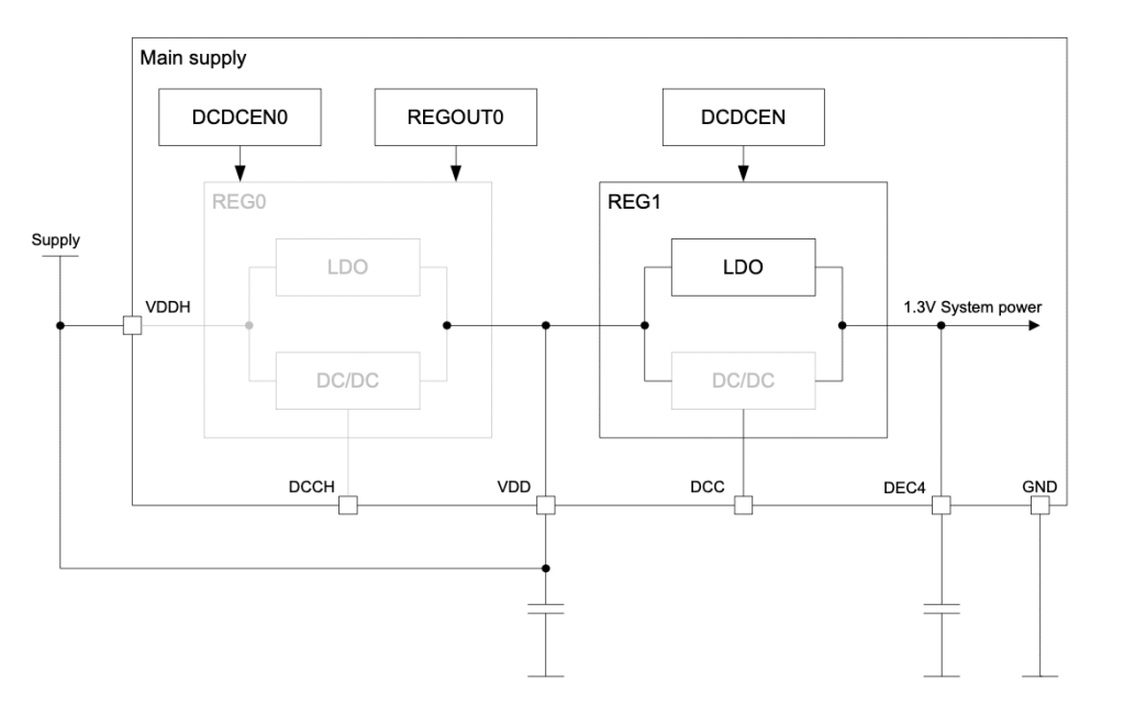
LimitedResults focused on DEC pins (DEC1, DEC2 until DEC6), where external decoupling capacitors are connected.
DEC4is the power line after the REG1 stage. So, it probably supplies the entire digital system (CPU & memories)DEC1is definitively the CPU power line.
PCB modifications
(for nrf52840) 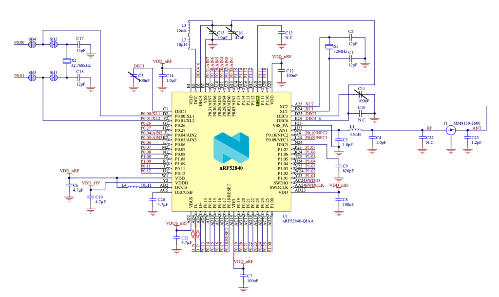
The corresponding decoupling capacitors C5, C15, C16 and C11 are removed.
Glitch window
In the next screenshot, the Arm CPU starts its execution (at 19us after the trigger mark). It is distinguishable on CH2 (CPU power consumption): 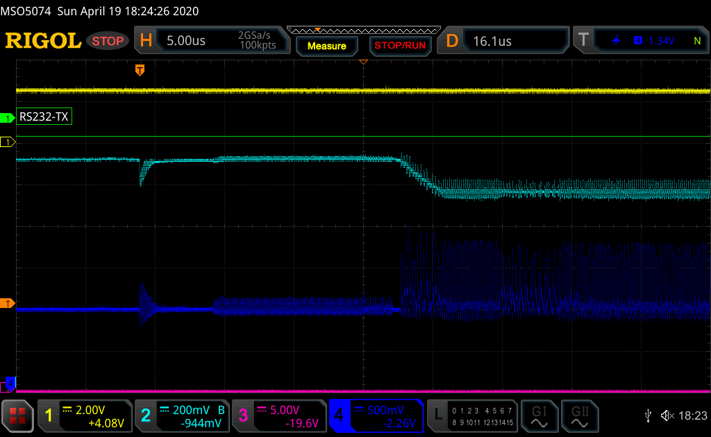 CPU starting its execution. CH1= UART, CH2 = CPU power(DEC1) and CH4= System Power(DEC4).
NVMC activity, by comparing the two power signals DEC4 and DEC1:
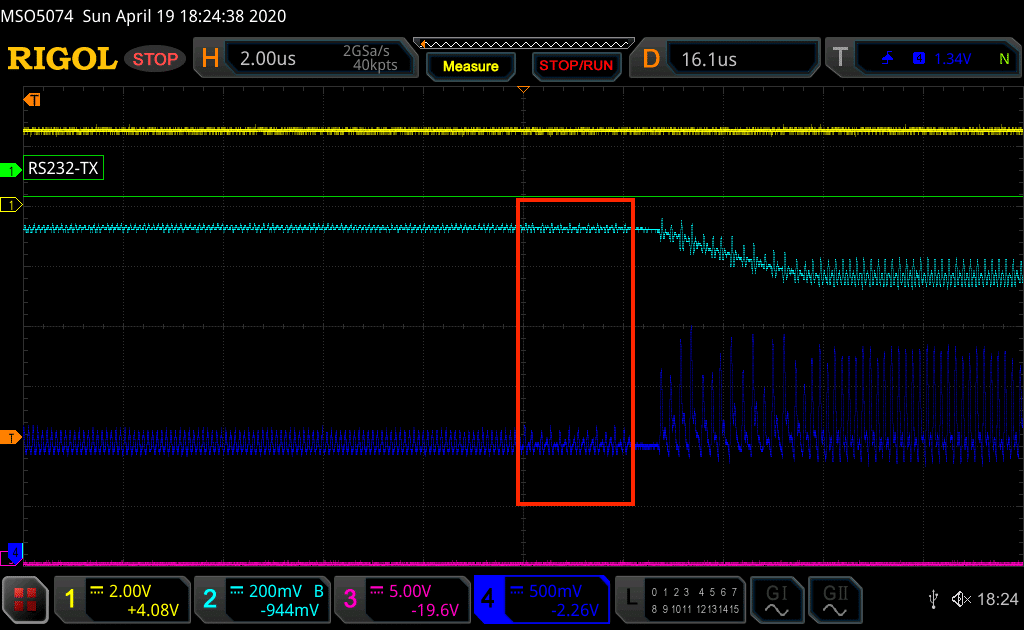 NVMC initialisation . CH1= UART, CH2 = CPU power(DEC1) and CH4= System Power(DEC4).
LimitedResults was able to identify that this pattern (red frame) corresponds to the memory controller (NVMC) transferring the UICR values to the core (or to the AHB-AP block directly) to configure the Debug Ports (AHB-AP, CTRL-AP) and set the APPROTECT to finally disable the debug interface.
Thus, this red frame is a target window for glitching.
Glitching Oculus Controller
Cause my main goal was to extract the firmware rather than focusing on the glitching technique itself, I aimed for simplicity and did not want to spend much time or energy on it. This was my goal, but reality hit me hard, and glitching the nrf52832 turned into a personal nightmare for me.
Rather than detailing my final successful attempt, I plan to walk through my significant steps/mistakes to provide a sort of “lesson-learned” perspective.
nRF52832 ref. design for reference: 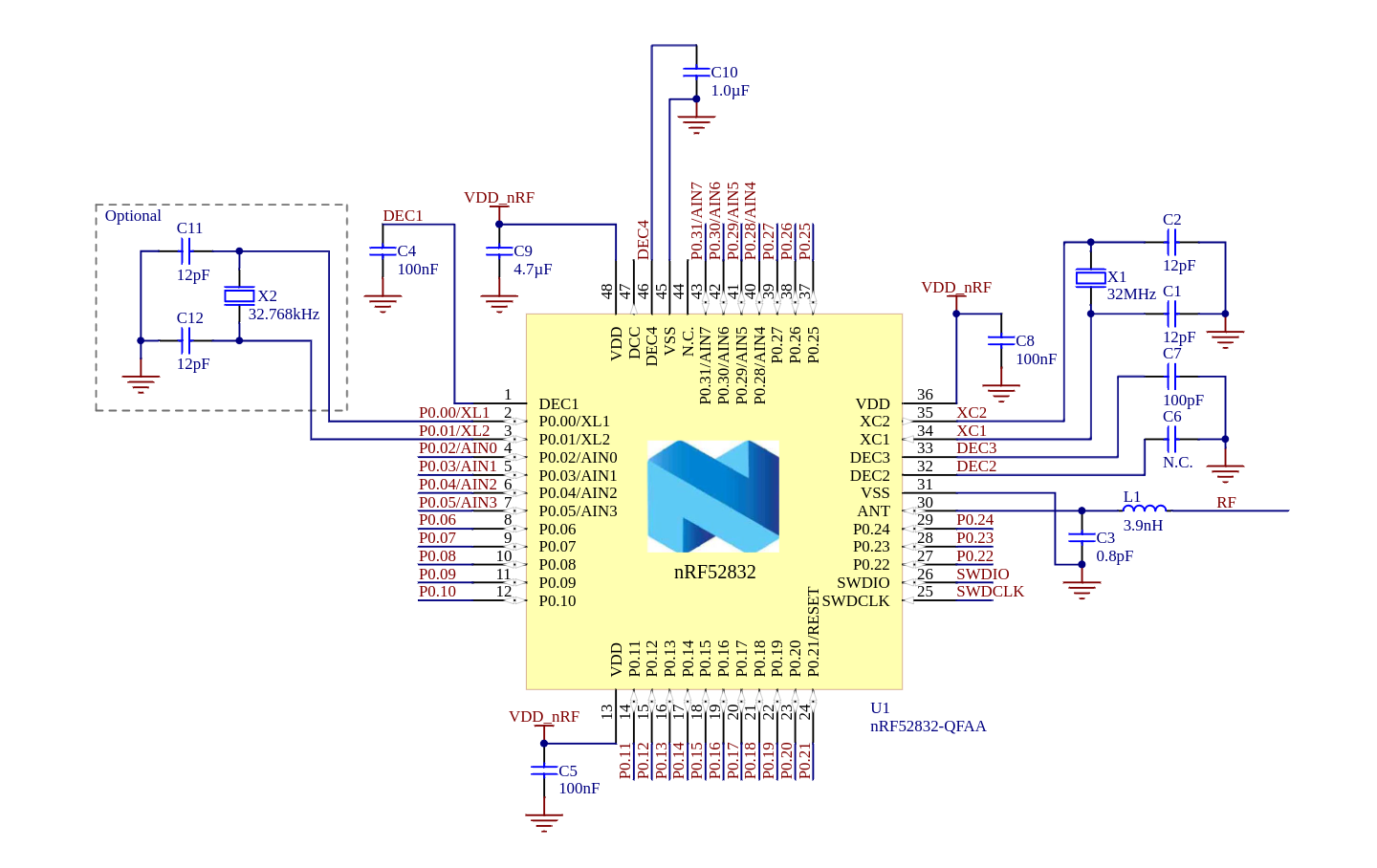
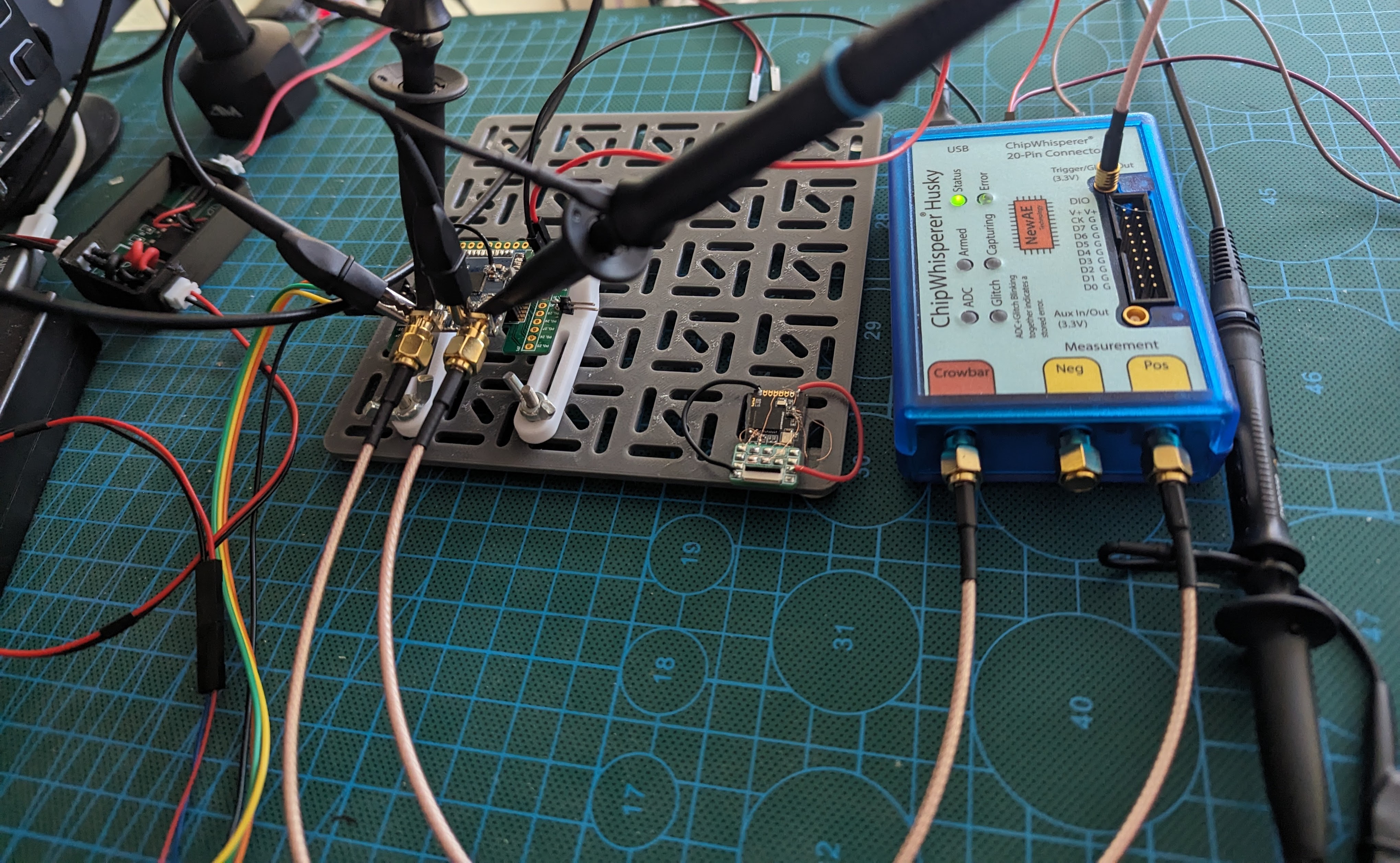
I chose the Chipwhisperer-Husky as my glitching tool. Having recently acquired the Husky, I hadn’t yet had the opportunity to use it. Therefore, this is my first attempt at utilizing it. Previously, I worked with the Chipwhisperer-Lite, but the Husky offers additional features and several differences, requiring me to essentially relearn most of the process from the beginning.
Segger J-Link Lite CortexM was used as a SWD tool.
Attempt #1
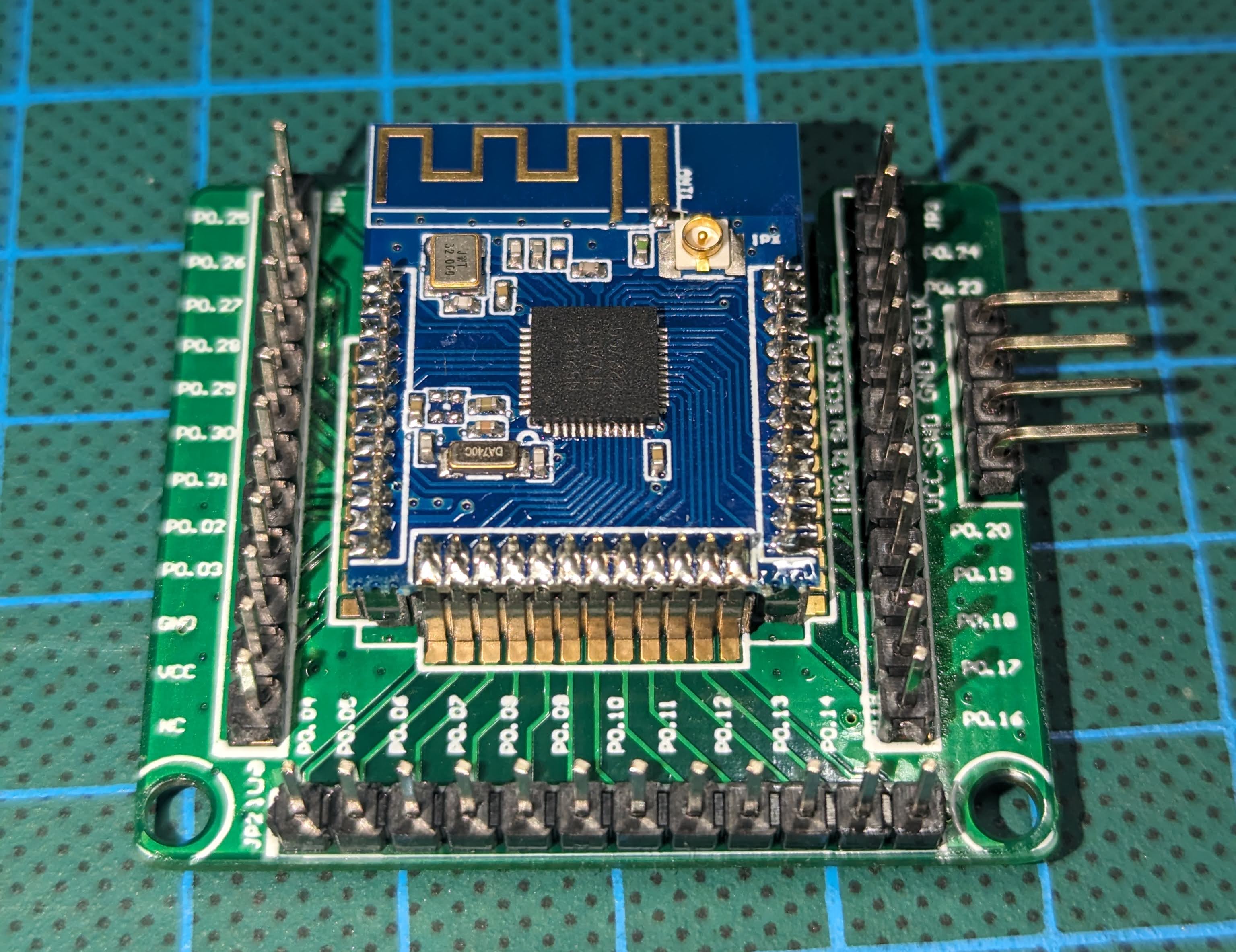
Before glitching the actual device, I decided to test the setup on a simple dev board.
I desoldered C4, C10, and C7 capacitors and soldered the glitch input to DEC1.
Because the original blog post does not describe glitching parameters (the trigger event, glitch delay, glitch pulse width), I used parameters from ESP32_nRF52_SWD project:
| glitch event | power on |
| delay (us) | 2000 - 30000 |
| pulse width (us) | 1-30 |
| power off delay (ms) | 50 |
| SWD wait delay (ms) | 100 |
HW modifications:
- capacitors C4, C10 and C7 are removed
- SMA connector to
DEC4 - Pin-header to
DEC1
The setup was the following:
- the target device was powered from chipwhisperer-husky GPIO (I used the nRST pin),
- the glitch wire was connected to
DEC1, - the trigger event - rise on nRST pin.
I tried to glitch using this setup for a few days but with no luck. I did go through Problems Glitching nrf52832 issue from ESP32_nRF52_SWD, changed parameters next, and ran for another couple of days:
| glitch event | power on |
| delay (us) | 7000 - 30000 |
| pulse width (us) | 1-60 |
| power off delay (ms) | 150 |
| SWD wait delay (ms) | 150 |
No luck :(
I gave up for a few weeks.
Attempt #2
I did everything the same as at the previous attempt but used hw from ESP32_nRF52_SWD instead of chipwhisperer-husky. The result was the same :(
Tried to use nrf52840-dongle as in ESP32_nRF52_SWD and again - no luck.
Attempt #3
This time I decided to dive deeper into the problem and understand the process in more detail. Following multiple experiments and measurements, I discovered that even a delay of 2000 microseconds is excessive for my board and the glitch pulse width is too wide.
Also, at this moment I was disappointed with the ESP32 solution and went back to using chipwhisper-husky.
Redo everything with next configuration
| glitch event | power on |
| delay (us) | 1200 - 2000 |
| pulse width (us) | 0.5 - 1.5 |
| power off delay (ms) | 150 |
| SWD wait delay (ms) | 150 |
HW modifications:
- capacitors C4, C10 and C7 are removed
- SMA connector to
DEC4 - Pin-header to
DEC1
No luck :(
Attempt #4
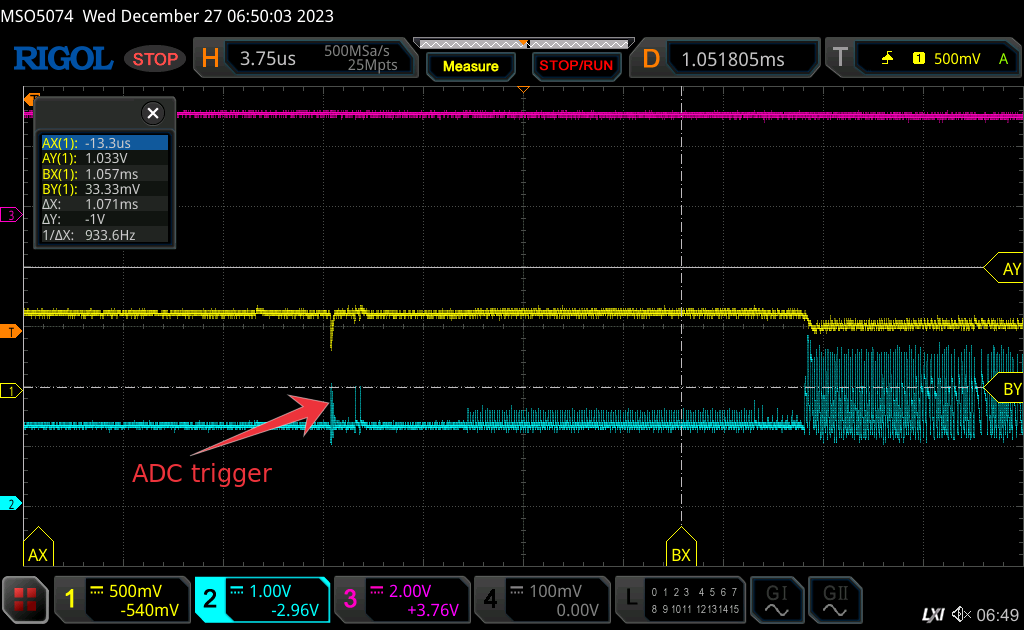
A key takeaway from the previous step is that using “power on” as a glitching event is ineffective. This is due to the “pattern” on the DEC4 line appearing at different times relative to the “power on” event. Thus, something more stable has to be used as an event. Chipwhisperer-husky has ADC, so as the event I decided to use the first “spike” on line DEC4.
Chipwhisperer-Husky’s ADC subsystem works a bit weirdly. I still do not fully understand how it works.
Redo everything with next configuration
| glitch event | ADC |
| delay (us) | 13.6 - 14 |
| pulse width (us) | 0.2 - 0.5 |
| power off delay (ms) | 150 |
| SWD wait delay (ms) | 150 |
HW modifications:
- capacitors C4, C10 and C7 are removed
- SMA connector to
DEC4 - Pin-header to
DEC1
and again… no luck :(
The main problem is that even ADC event is unstable and floating a bit, which is sufficient to prevent the glitch pulse from hitting the “target window”.
Attampt #N
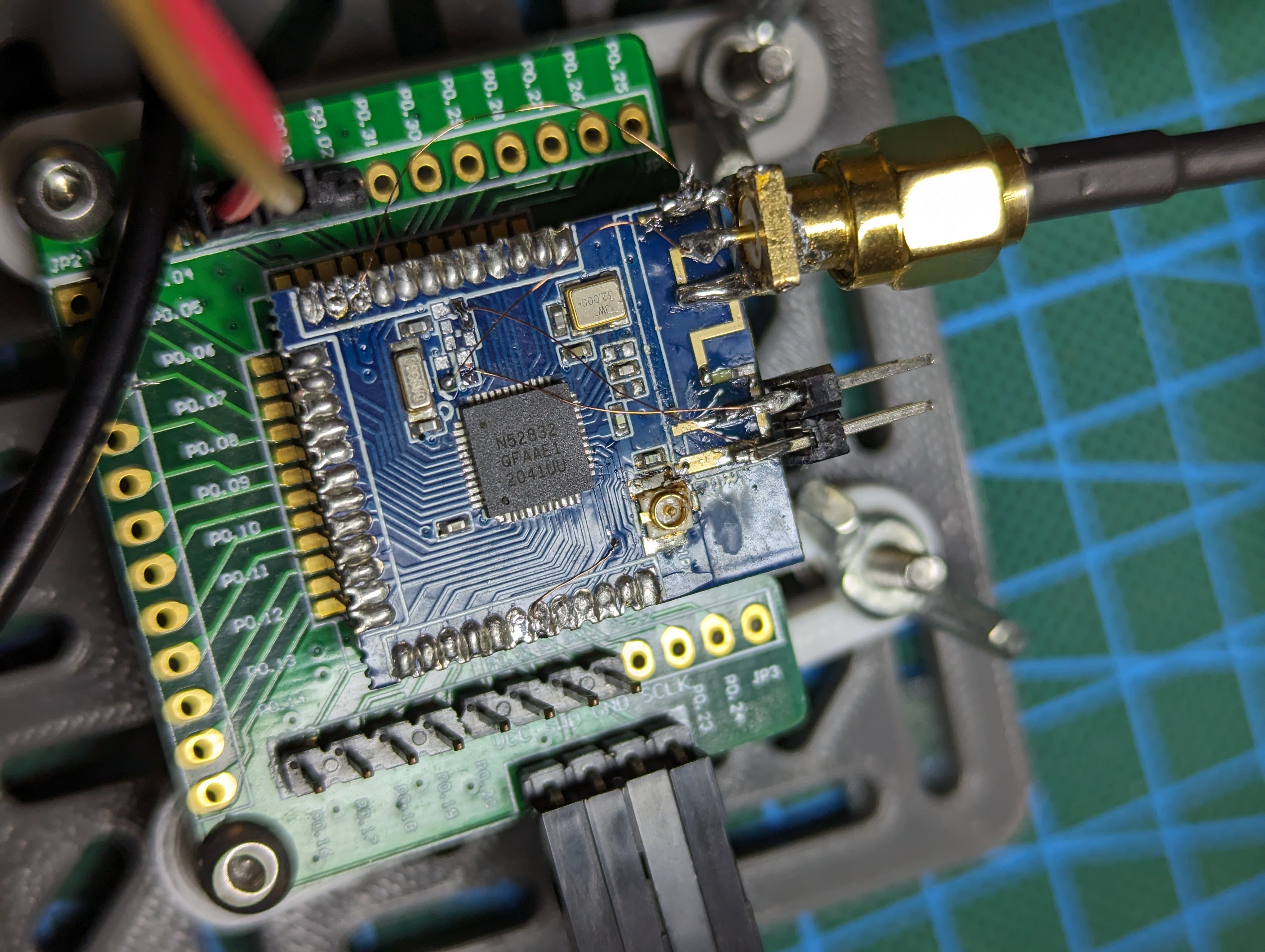
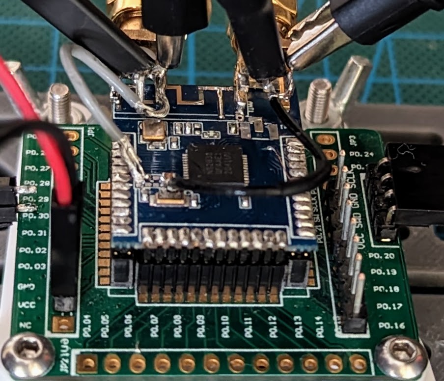
I did numerous tests, experimenting with various wires to connect the DECx line to an SMA connector (I also replaced the pin header for DEC1 with an SMA connector) and determining which capacitors should be removed and which should remain.
Eventually, I concluded that because glitching the test board proved challenging, attempting to glitch the controller board would likely be even more complex. Therefore, I decided to desolder the SoC from the controller board and put it on the test board to continue my experiments with glitching.
At some point, the test board looked like this:
a-a-a-a-a-and… I FINALLY DID IT!!!
I was able to bypass the readout protection and dumped firmware and UICR from Oculus 2 controller.
The modifications that changed everything and led me to success were:
- Soldering back all capacitors except for C10, which is on the
DEC4line. - Using a thin RF cable (cut from an SMA to u.FL RF Adapter Cable) to connect
DEC1andDEC4to SMA connectors.
Configuration:
| glitch event | ADC |
| delay (us) | 13.6 |
| pulse width (us) | 0.2 |
| power off delay (ms) | 150 |
| SWD wait delay (ms) | 150 |
Husky setup:
1
2
3
4
5
6
7
8
9
10
11
12
13
14
15
16
17
18
19
20
21
22
23
24
25
26
27
28
29
30
31
32
33
34
35
36
37
38
39
40
        scope = cw.scope(name='Husky')

        scope.reset_fpga()

        scope.clock.clkgen_src = 'system'
        scope.clock.clkgen_freq = freq
        scope.clock.adc_mul = 1
        scope.clock.pll.update_fpga_vco(600e6)

        scope.trace.enabled = False

        scope.glitch.enabled = True
        scope.glitch.clk_src = 'pll'
        scope.glitch.output = "enable_only"
        scope.glitch.trigger_src = 'ext_single'
        scope.glitch.width = scope.glitch.phase_shift_steps // 2
        scope.glitch.repeat = 1
        scope.glitch.ext_offset = 0

        scope.io.glitch_lp = False
        scope.io.glitch_hp = True
        scope.io.hs2 = 'glitch'
        scope.io.glitch_trig_mcx = 'trigger'

        scope.trigger.module = 'ADC'
        scope.trigger.level = -0.1

        scope.adc.timeout = 3
        scope.adc.offset = 0
        scope.adc.basic_mode = 'rising_edge'
        scope.adc.clip_errors_disabled = True
        scope.adc.lo_gain_errors_disabled = True

        scope.gain.db = 20
        scope.adc.bits_per_sample = 12
        scope.adc.samples = 2*2**16
        scope.adc.presamples = 10000

        scope.io.nrst = False
        scope.io.target_pwr = True
I don’t have a range set in the “delay” section of the configurations for the reason: With the current setup, I achieved a high success rate, making a range unnecessary. The success rate is approximately 70% and nearly every run results in a successful glitch.
This configuration works for me, and with high probability will not work for you out of the box because parameters are very setup specific(depends on board, power, wires and so on).
More photos
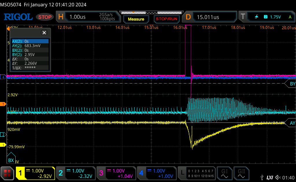
- Final HW setup
- Successful glitch captured on the scope!
Summary(lessons learned)
- There are no out-of-the-box solutions for HW fault injection.
- Patience is absolutely crucial—and you need a lot of it!
- HW fault injection(yeah, I think, in general, any research) is time-consuming.
- The type of wires matters.
- Achieving stable power is challenging.