Inside the Oculus3 Controller: A Closer Look
Intro
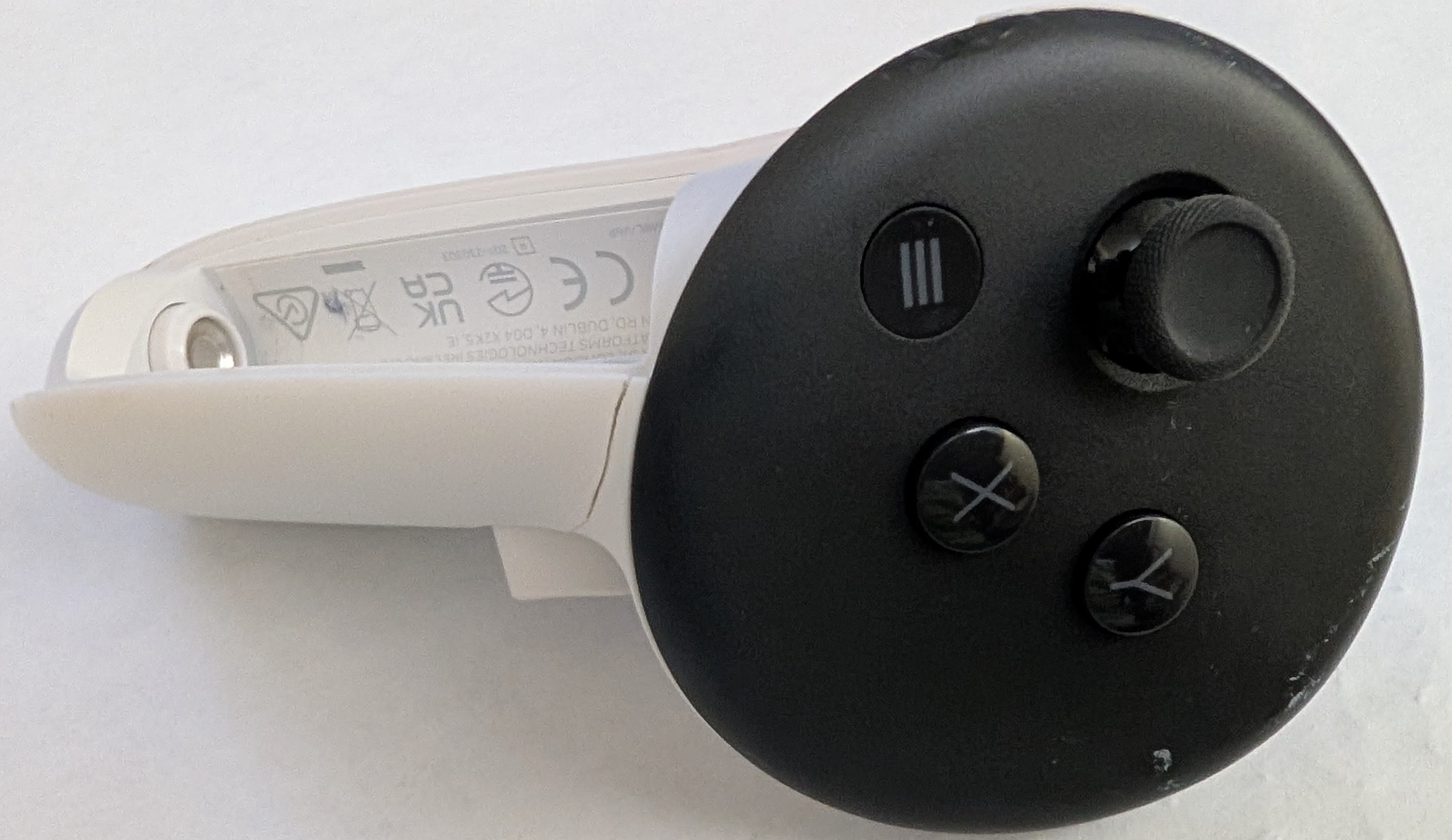
I recently got my hands on a controller from the Oculus Quest 3 and decided to explore what’s new.
The Oculus Quest 3 controller brings several hardware updates from its predecessor, the Quest 2, most notably the switch to newer MCUs (microcontroller units). This post dives into some of my findings during a recent teardown and reverse engineering process.
Teardown
Major Hardware Changes: NRF52820 and ATSAMD21G
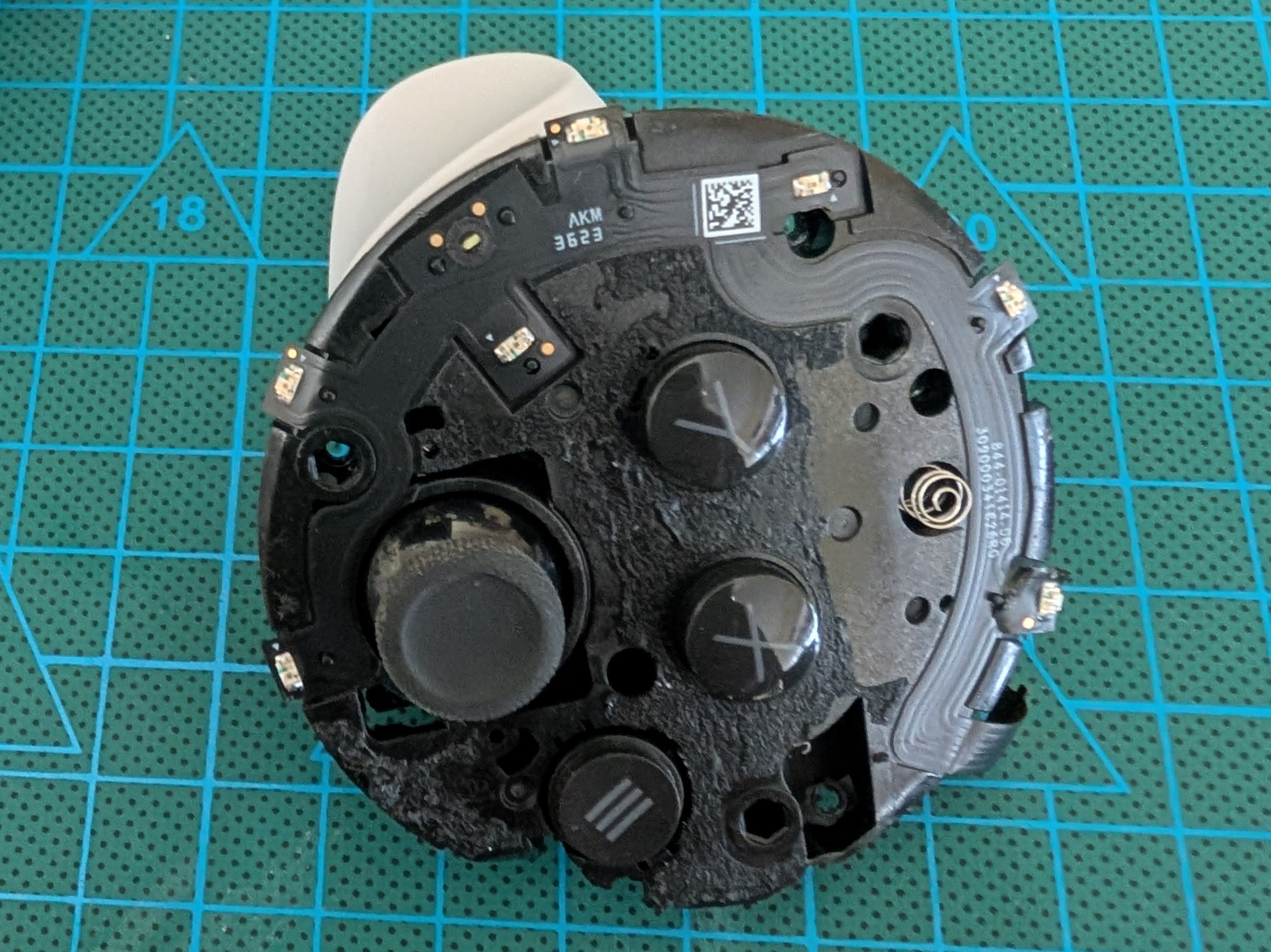
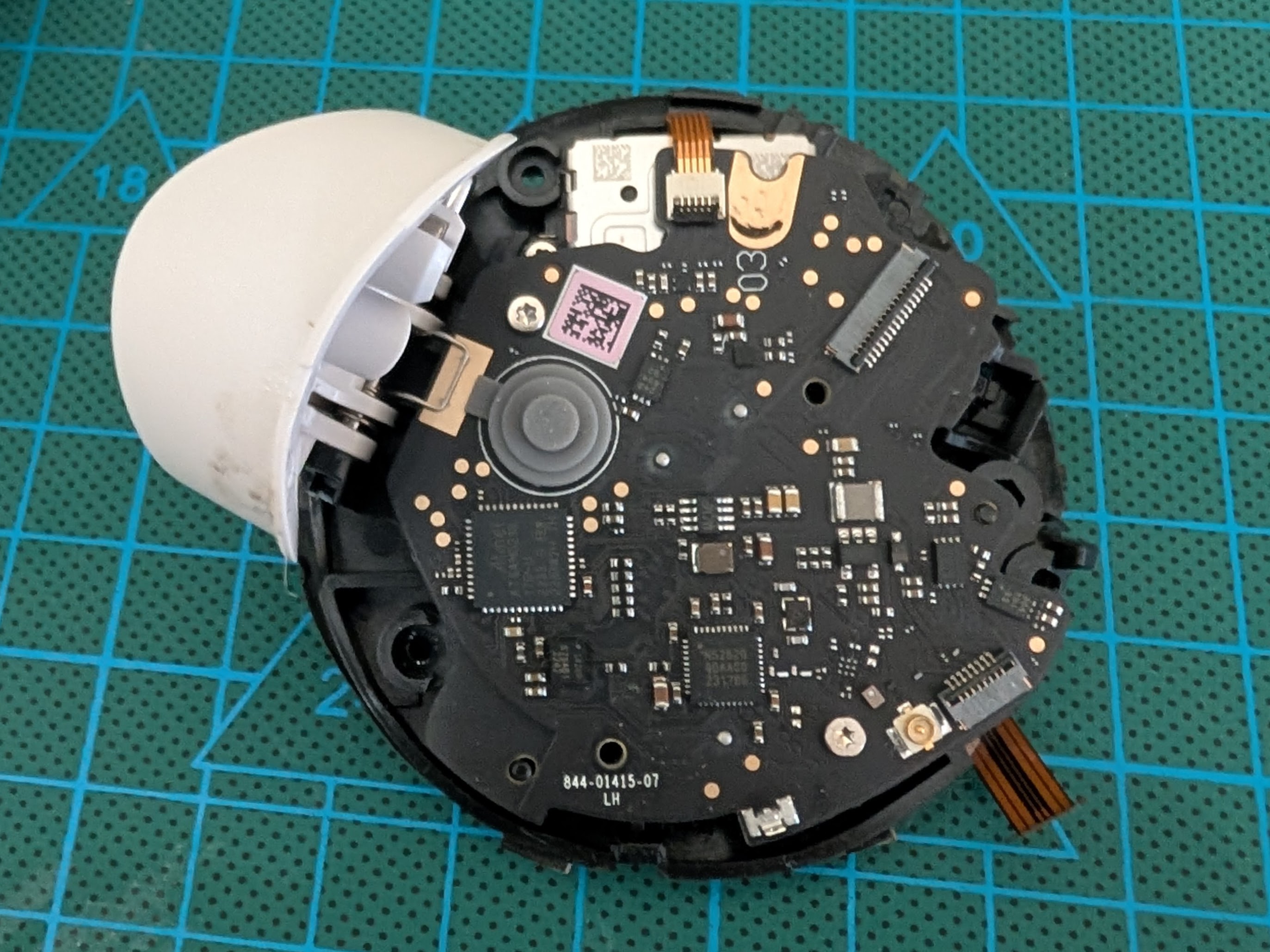
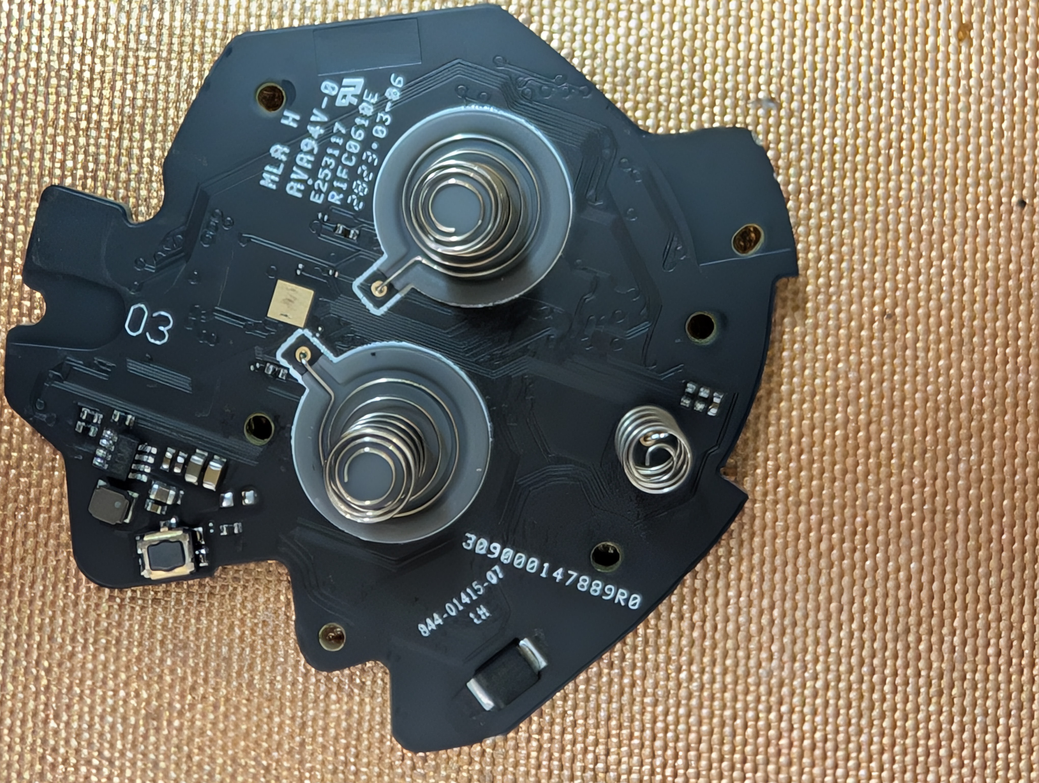
From the photos above, a significant change is apparent in the new controllers. Oculus has transitioned to different MCUs:
nRF52820 has replaced the nRF52832. Both are Bluetooth Low Energy (BLE) SoCs from Nordic Semiconductor, but the nRF52820 is more power-efficient and designed to fit smaller form factors, ideal for wearables and handhelds like controllers.
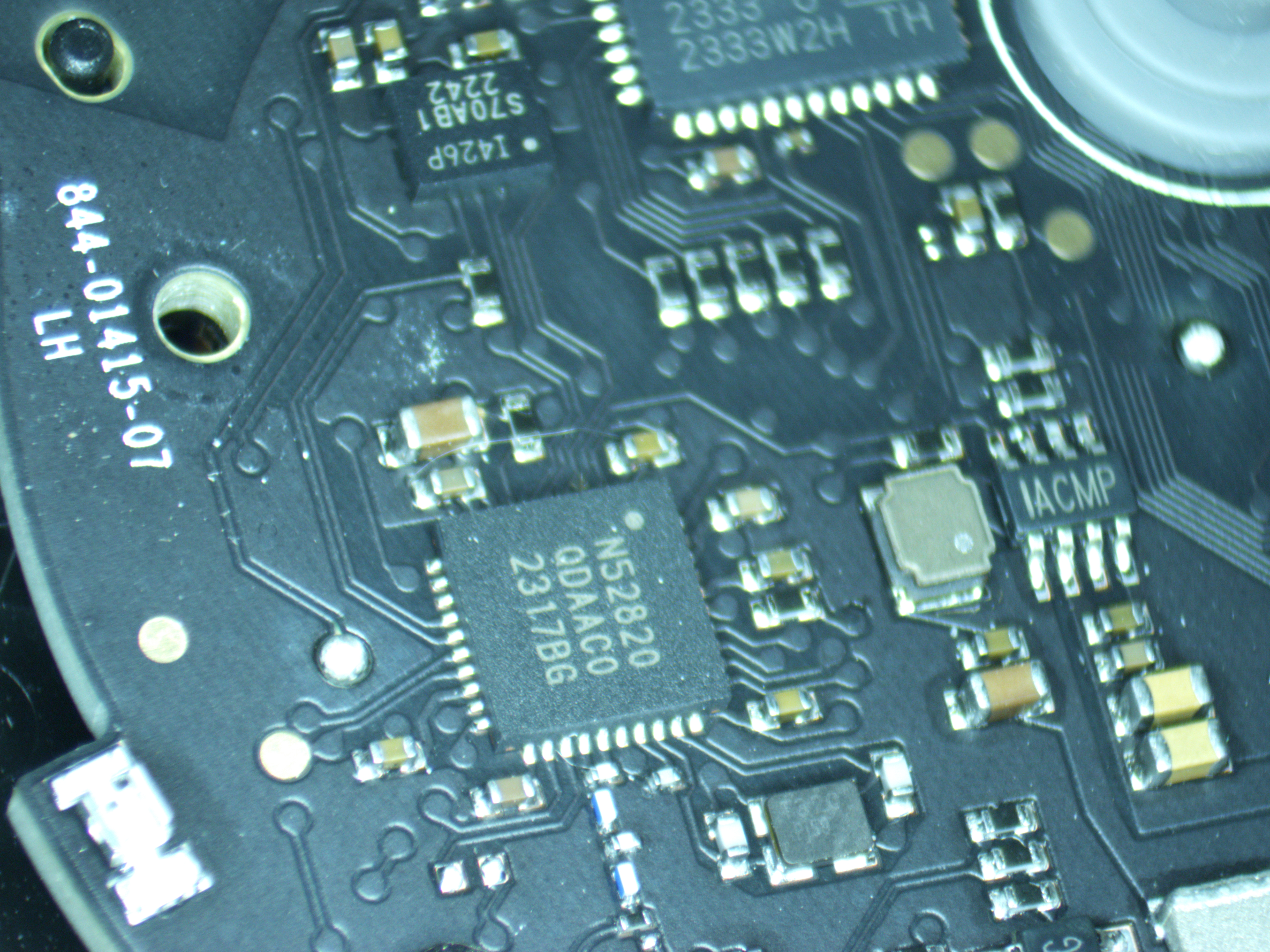
ATSAMD21G now takes the place of the ATTiny1616. This microcontroller is known for its higher performance, increased memory, and better power efficiency, which is likely used for secondary functions in the controller.
The shift to these MCUs suggests improvements in power management and enhanced controller responsiveness.
Reverse Engineering the PCB: Tracing the Connections
In the teardown, I examined two key PCBs in the controller. Here’s a breakdown of the reverse-engineering process and the information gathered, as shown in the annotated photos.
1. Main Board
The most of the components are assembled only on one side, which is accessible after detaching the “handle” from the “head” of the controller.
The top side of the main board reveals several pads and tracks that I’ve traced out, marked in red. Important highlights include: 
SWD (Serial Wire Debugging) points for both the nRF52820 and the ATSAMD21G. These pads (SWDIO, SWCLK, etc.) allow for hardware debugging and flashing firmware, which will be essential for anyone looking to modify or further investigate the firmware of the controller.Most likely, the SWD is disabled on production units, so a hardware attack (such as glitching) may be necessary to gain access to the firmware.
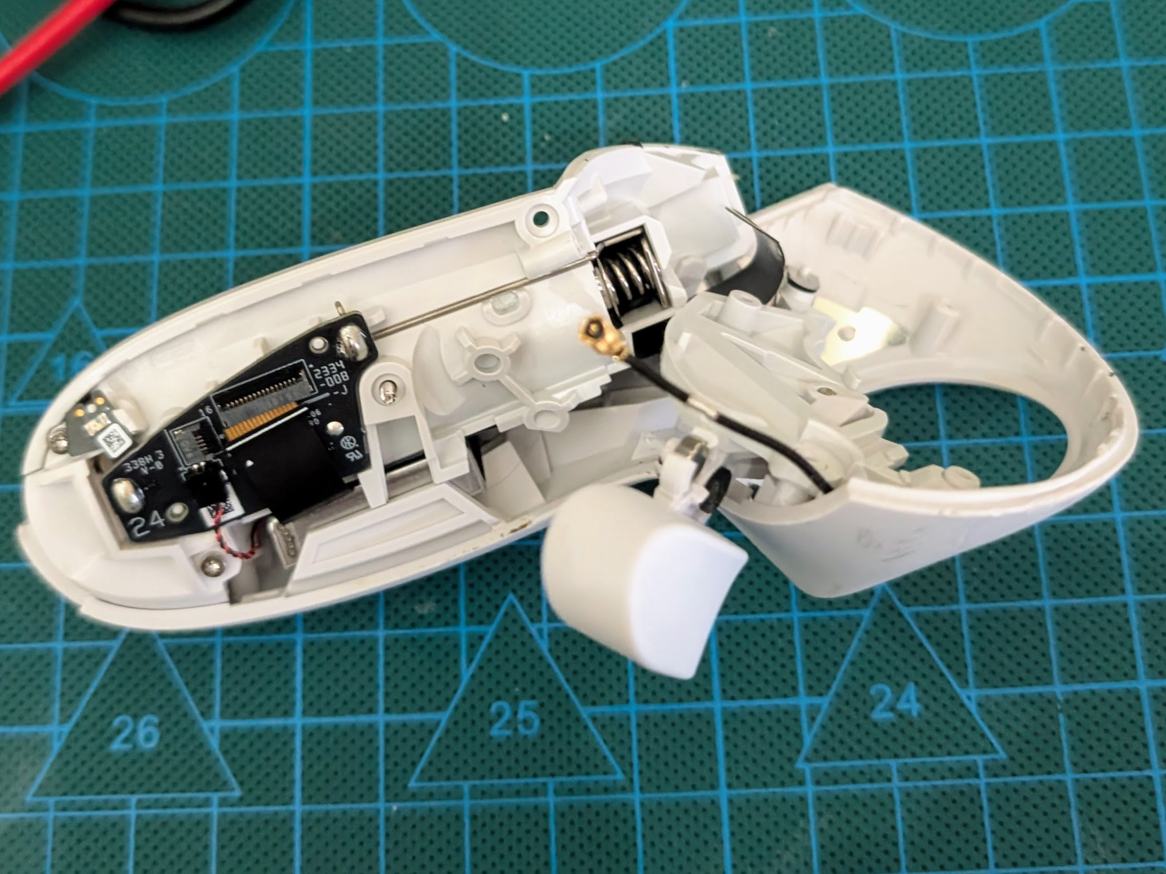
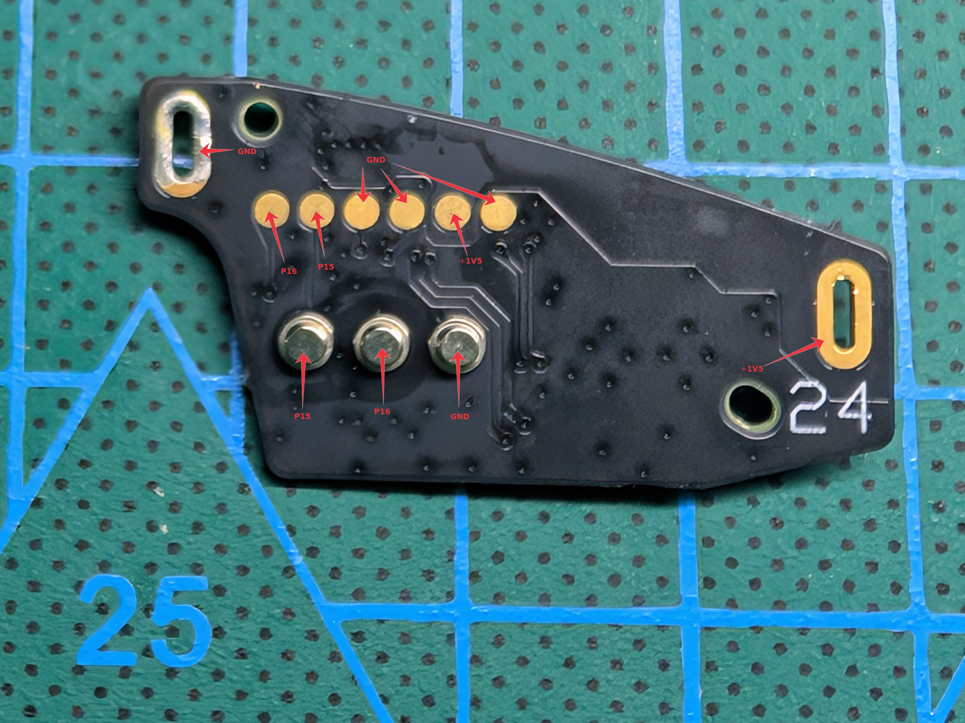
nrf52 P0.28 and P0.29 ping are routed down to handle board (p15 and p16 of flex cable) and are accessable from battery tray without a controller disassemling. I guess these pins are utilized for some form of debugging.
The signal appears to be UART at 115200 bps, but the output isn’t a standard string; it looks like xA5Z\x01\x02@\x01\x9C\xFA. Therefore, I’m not entirely certain.
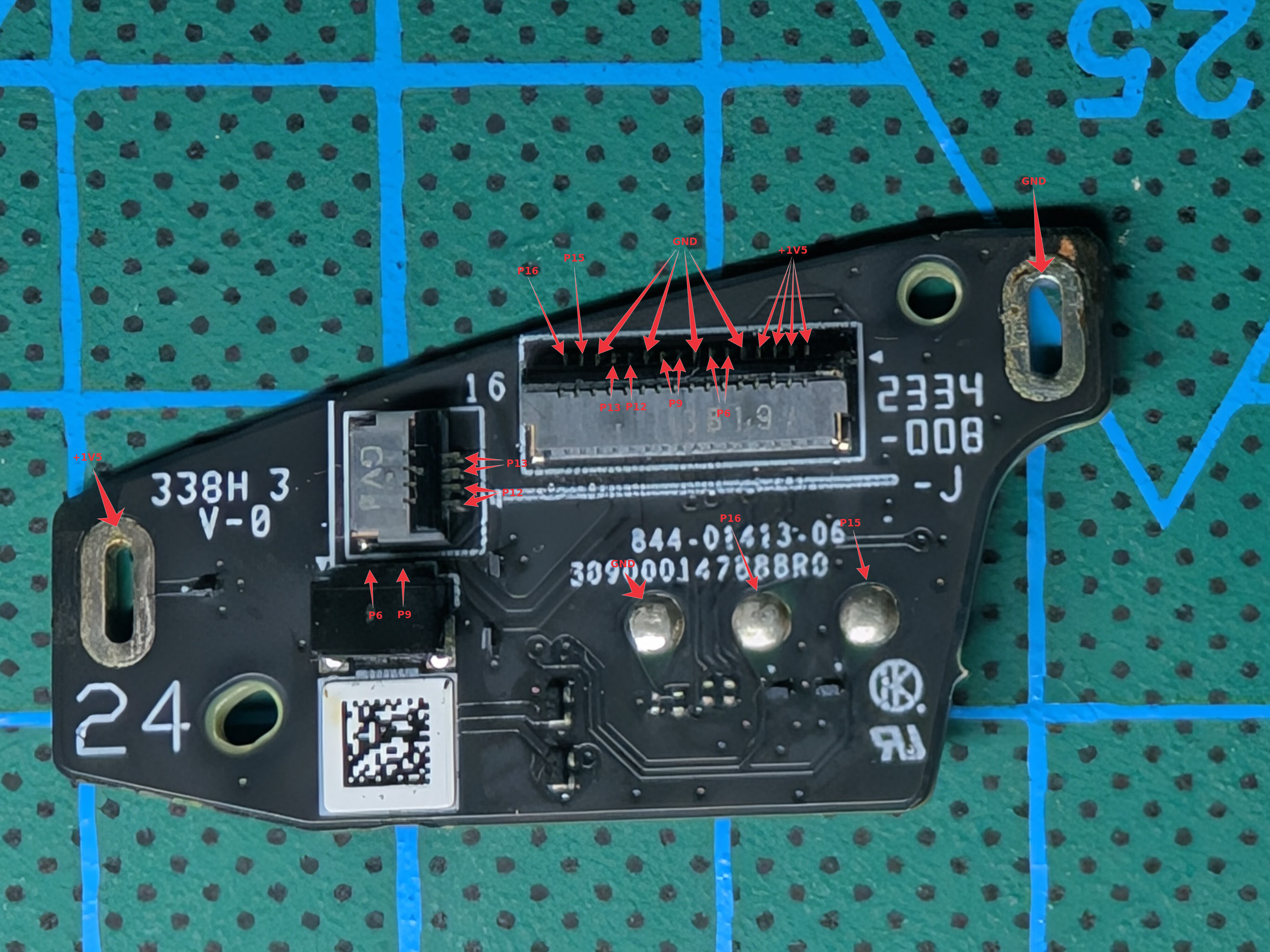
2. Handle Board (Top and Bottom)
The secondary board, near the battery, showcases additional crucial pads and wiring for power regulation:
P15 and P16 Pins: These pins connect to the nrf52 MCU (P0.28 and P0.29) and are likely utilized for some form of debugging.
Power and Ground Tracing: Like the main board, several GND and +1V5 (1.5V) power lines are identified, responsible for delivering power to the board’s components.
Flex cable pinout
| #pin | desc |
|---|---|
| 1 - 4 | +1.5V |
| 5 | GND |
| 6-7 | Motor+ |
| 8 | GND |
| 9-10 | Motor- |
| 11 | GND |
| 12 | LED+ |
| 13 | LED- |
| 14 | GND |
| 15 | nrf52 P0.28 |
| 16 | nrf52 P0.29 |
Conclusion
The Oculus Quest 3 controller, featuring MCUs like the nRF52820 and ATSAMD21G, presents an interesting opportunity for reverse engineers. The identified SWD and possible UART points offer the potential to read or modify the firmware, opening doors for custom software development or further investigation into the controller’s internal workings. These insights provide a solid foundation for exploring the device further, including its BLE functionality, which I plan to cover in future posts.
If you’re working on similar hardware or have insights to share, feel free to reach out!
